Best Spring Test Probes China Manufacturer For IC Testing
Spring test probes test IC chip and contact chip testing points accurately, with high stability, durability, wear resistance, reducing poor contact. Gold-plated beryllium copper & tungsten alloy for semiconductor test, electronic production lines and R&D to test BGA, QFN, CSP, etc. Johoty offers complete custom.
Features:
- High precision contact, accurate signal transfer.
- Quality materials, resistant to temperature and wear.
- Stable spring force reduces testing errors.
- Widely compatible with various IC packages.
- Durability, long lifespan, reduced maintenance.
- Customize specifications to meet diverse needs.
Spring Test Probes Series
Spring test probes are dual head double action to connect testing instruments and IC testing points, use gold, beryllium copper, tungsten alloy, designed as pointed, round, claw head, etc. Use music steel and stainless steel to design springs with spring force from 15gf to 500gf. Gold plating, palladium, platinum, etc., get a contact resistance >1m Ω. Includes micro, high-speed, low impedance, adjustable spring force, etc. Customize dimensions, materials, spring force, IC pin pitch, layout, current, coating, and more. Johoty can flexibly customize performance, balancing durability and price.
Function of Spring Test Probe for IC Test
Parts | Function |
---|---|
Plunger Tip | Directly in contact with IC pins/pads/bumps, common shapes include conical, flat, crown, blade-shaped, spherical, etc. Raw material is generally tungsten alloy SK4, Cobalt alloy, finishing with gold plating, rhodium plating, nickel plating, etc. |
Spring | Provide constant contact force within compression stroke, made of materials SUS304, SUS631, nickel titanium alloy (NiTi), etc., spring range covers 5gf -150gf. Custom. |
Barrel | Shell guide element, maintaining plunger’s linear axial movement. Usually made of brass, phosphor copper, or stainless steel, with an outer layer of gold or nickel plating to prevent oxidation. |
Specifications of Spring Test Probe for IC Test
Parameter | Range & Technical Remarks |
---|---|
Contact Resistance | 15–100 mΩ, Custom. Lower values improve signal fidelity in high-speed tests |
Max Current Rating | 1.0–8.0 A, Custom. dependent on pin core diameter and plating material (e.g., gold over copper) |
Max Operating Voltage | 1–500 VDC, Custom |
Spring Stroke | 0.10–6.00 mm, Custom. Typical range 1.0–3.0 mm for stable contact and lifespan |
Spring Force | 5–300 gf, Custom. 50–120 gf recommended for most IC probing scenarios |
Tip Diameter | 0.10–1.27 mm, Custom. matches most industry socket standards |
Barrel Diameter | ≥0.12 mm, Custom. affects PCB drill size and pitch compatibility |
Minimum Center Pitch | 0.3–1.0 mm, custom. critical for QFN, BGA, WLCSP fine-pitch testing |
Operating Temperature | -40°C to +120°C, suitable for thermal stress and aging tests |
Cycle Life | 50,000–1,000,000 insertions, material fatigue resistance indicator |
Plunger Tip Style | Conical, blade, dome, crown types, selected by DUT pad geometry |
Surface Plating | Gold, silver, Pd, Pt, Ru, Rh, or nickel, impacts resistance stability and oxidation |
Plunger Tips of Spring Test Probe for IC Test
Plunger Tip Shape | Advantages | Targets |
---|---|---|
Conical | Strong pierce | Oxidized surfaces |
Spherical | Low wear | Balls/FPC |
Flat | Even force | Copper/metal |
4-Point Crown | Multi-contact | BGA bottom/rough |
6-Point Crown | Mid-array | BGA/LGA |
9-Point Crown | High-stability | Chips/arrays |
Blade | Cuts oxide | Aluminum/aged pads |
Fork | Firm grip | Micro pins |
Spiral | Self-cleaning | Repeat points |
Cylindrical | Easy align | Vias/probe bases |
Angled | Easy insert | Slanted contacts |
Concave | Stable align | Micro holes/posts |
Oval | Wide contact | Soft pads |
Diamond | Self-aligning | BGA/irregular holes |
T-Head | Lateral hold | Side pads |
Blade Tip | Penetrates | Coated lines |
Wavy | Anti-slip | Coated metal |
Disc | Rotational | Rotating points |
Slotted | Locked hold | Slotted pins |
Applications of Spring Test Probe for IC Test
Automatic Test Equipment (ATE) system: connect test motherboard with IC under test for signal integrity and low contact resistance, improving test accuracy and system throughput.
SoC system level testing platform: used for high-speed signal acquisition and stable power injection, achieving multi-channel parallel testing. It’s to ensure the reliability of the system level verification phase.
Wafer Level Test: accurately contacting the wafer pad with micro dual head probes. High-density probe arrangement and stable mechanical rebound are achieved, supporting automated probe station operations.
Final Test: During the finished product packaging testing phase, ensure that the pin functionality and electrical performance meet specifications. Spring test probes have wear resistance and high repeatability characteristics.
High frequency communication chip testing: Conduct high-frequency signal injection and reception testing on RF/5G chips. Requiring probes to have extremely low insertion loss and precise impedance control capabilities.
Memory chip testing (DRAM/NAND): used for high-speed IO interface testing, such as DDR4/5, requiring probes to have nanosecond response speed and stable contact capacitance control.
Automotive Electronic Chip Testing (AEC-Q100): Testing the reliability of automotive grade chips under high and low temperature/high vibration conditions. With probes that are corrosion-resistant, have a long lifespan, and support dynamic contact loads.
Power IC testing: used in high voltage and high current applications. the probe needs to withstand a current of 20A or more and maintain low thermal resistance to avoid local overheating.
Programmable Logic Device (FPGA/ASIC) Verification: Used for fast programming and verification stages. With multi-channel parallel connections, probes that support high-frequency signals and precise logic level recognition.
Multi Chip Module (MCM) Testing: Joint functional testing of multiple chip modules in heterogeneous packaging. Requiring probes to maintain good coplanarity and pressure consistency in dense spaces.
Bio electronic chip testing (Lab on Chip): suitable for ultra-small signal detection and analog interface testing. the probe needs to have micro Newton level contact control and extremely low noise interference characteristics.
Defense/aerospace grade chip certification testing: used to meet the MIL-STD certification process, the probe needs to pass reliability verification in extreme environments such as high acceleration, high altitude, and strong radiation.
Why Choose Johoty's Spring Test Probes?
Johoty’s spring test probes are high-precision, highly stable testing solution. Meet different IC chip packaging, precise conductivity, low resistance, improved testing efficiency. Fast delivery, high cost-effectiveness, Johoty is trustworthy.
Packaging of Spring Test Probe for IC Test
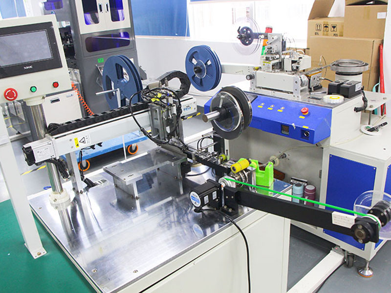
Adapt to the universal size of positioning holes for burning fixtures
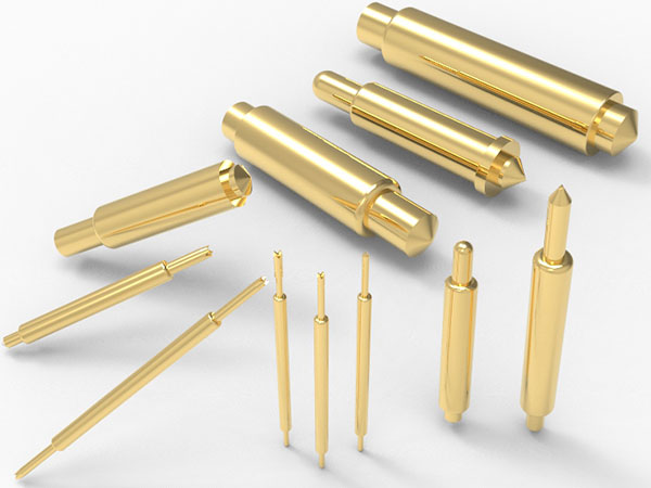
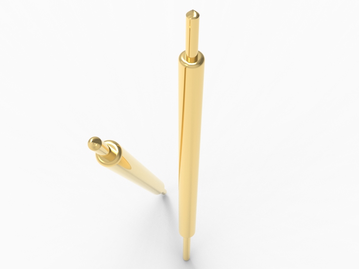
Outer diameter design of the tail of the Spring Test probes follows the spacing between the needle holes of the dual main flow fixture of 0.635mm and 1.27mm. Compatible with most main control chip burning platforms. The positioning deviation should be controlled within ± 0.02mm. Ensure high plug consistency and repeat positioning accuracy even in multi probe array arrangements.
Probe module supports multi package alignment requirements
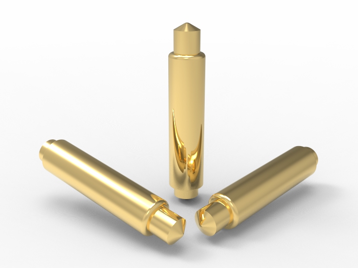
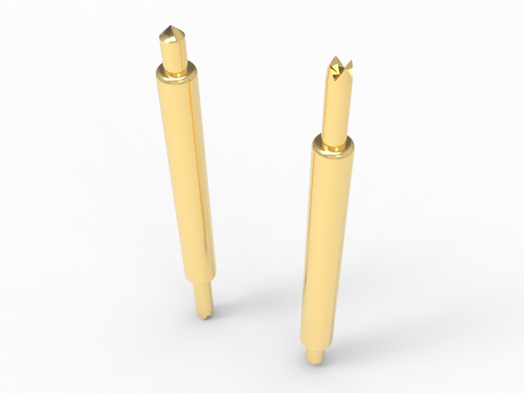
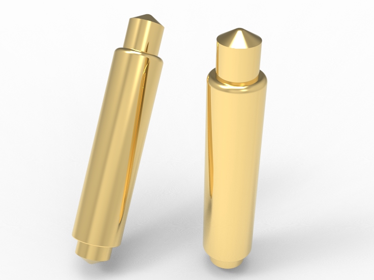
The front-end plunger tip can be selected with cone head, hemisphere, blade type and other structures, suitable for SOP, QFN, BGA, etc. The packaging spacing covers the range of 0.3mm to 2.54mm, and the central axis error is controlled to be less than 10 μ m. It meets the rigid tolerance requirements of the automatic alignment platform for precise contact.
Uniformity and interchangeability of module structure dimensions
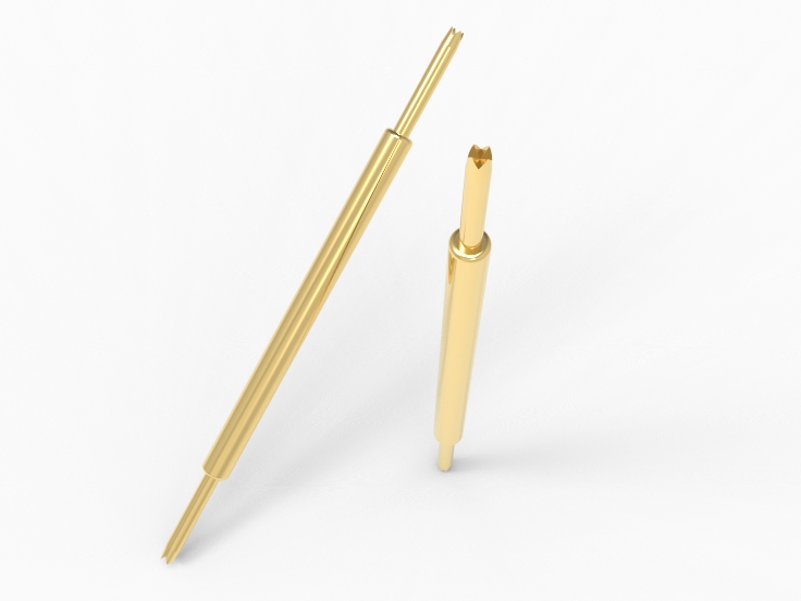
Total length of Spring Test probes can be customized between 16mm and 33mm, and is compatible with mainstream burner head structures. All modules adopt a unified guiding structure and stop limit to maintain assembly consistency. The elasticity specification is within the range of 20gf to 150gf, and the repeated compression life exceeds 300,000 cycles.
Standardization and maintainability of supporting accessories
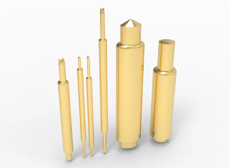
Optional standard components include limit rings, guide tubes, buffer springs, etc. The outer diameter of the components is uniformly divided into two sizes: Ø1.02mm and Ø1.36mm. Easy to quickly adapt to the burning probe holder. All accessories support tool free replacement, increasing maintenance efficiency by over 32%. Suitable for quickly changing requirements in continuous testing environments.
Quality and Test of Spring Test Probes for IC Test
Probe spring lifespan: The standard lifespan requirement is ≥100,000 cycles, and for critical applications it is ≥300,000 cycles. It needs to be verified through cyclic compression testing, and the load stability and coefficient of variation CV value should be recorded to be ≤5%.
Initial contact resistance: The standard requirement is ≤ 50mΩ, measured using a 4 wire testing method. Multi point measurement, the average value needs to meet the process stability assessment (CPK ≥1.67).
Material consistency: Barrel, springs, and plunger must be made of factory-certified materials (such as BeCu gold-plated or SK4 high carbon steel). Attached are RoHS/REACH compliance certificates and material spectral analysis data.
Coating thickness and uniformity: The standard for gold coating thickness is ≥1.27μm (50μin), and XRF detection is used. Thickness deviation ≤ ±15%, to avoid poor contact caused by local thinning.
Dimensional tolerance control: All critical dimensional tolerances are controlled within ±0.05mm. Batch sampling is conducted using high-precision digital projectors and automatic optical measurement systems.
Batch consistency verification: SPC statistical analysis is required for each batch, and key parameters (such as spring force and resistance) meet the 3σ control limit requirements. Abnormal batches shall not flow into subsequent processes.
Corrosion resistance: It needs to pass a salt spray test (96 hours, 5% NaCl), and after the test, the contact resistance increases by ≤10%, and the coating has no visible corrosion spots.
Plunger tip shape control: The plunger tip structure should comply with the design parameters (A type, B type, H type, etc.), and the precision of the sharp angle R should be controlled to be ≤±0.005mm. Microscopic inspection ensures no burrs or cracks.
FAQ
What is Function of Spring Test Probes?
Spring test probes are tools for testing IC chips. Test probes help establish connections between chips and devices. Ensure accurate transfer of electrical signals. Suitable for high-density packaged chips. Widely fit mass production testing.
What are Advantages of Spring Test Probes?
Accurate contact can improve efficiency. Long lifespan reduces replacement costs. Spring test probes are compatible with various chip packaging types. Easy to operate or handle, and very convenient for large-scale use. Stable performance improves testing reliability.
What is Lifespan of Spring Test Probes?
It is usually 100,000 cycles, common lifespan of 200,000 times. Use frequency will affect the lifespan. Extend life cycles by scheduled cleaning and maintenance. Choosing high-quality materials can improve lifespan. Johoty’s spring test probes have more reliable lifespan.
How can Spring Test Probes Ensure Reliable Test Results?
Improve signal quality through precise contact. Reduce contact resistance interference on circuit stability. Highly conductive materials ensure superior performance. Structural design prevents signal attenuation or distortion. Strict manufacturing ensure consistency.
What Testing Environments are Spring Test Probes Suitable For?
Can work normally in high and low temps. Support the demand for transmitting high-frequency signals. Can adapt to various current and voltage. Compatible with manual and automated testing equipment. Suitable for complex chip testing requirements.