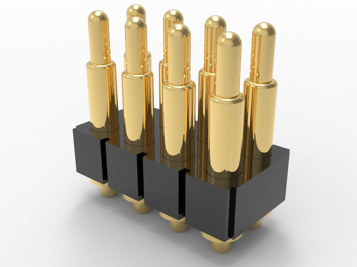
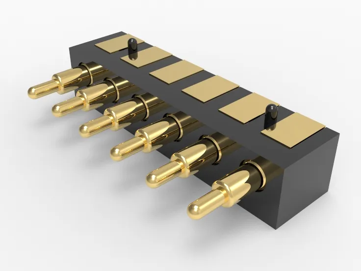
Johoty’s Services of PCB Pins
Prototype PCB Pins: A fast prototyping development channel that takes 10-15 days to complete high-precision prototyping. No need to repeatedly confirm drawings, dedicated FAE engineers provide one-on-one technical follow-up throughout the entire process. Ensure that the zero resistance trial run is immediately validated upon receipt.
Quality assurance: Military grade reliability, with a lifespan of up to 100,000 insertions and removals. 100% full inspection for shipment, with precision tolerance control of ± 0.05mm to ensure stable connection and reliable conductivity. Meet strict standards (RoHS/REACH/UL).
PCB Pins delivery efficiency: Standard inventory is delivered within 3 days, customized products are produced and delivered within 2 weeks. Rapid response to engineering scheduling, adapting to the full cycle requirements from research and development verification to mass production import.
Minimum Order Quantity (MOQ): Sample size as low as 5pcs, mass production MOQ of 3,000pcs, supporting multi specification mixing. Small batch validation, fast decision-making without threshold, reducing the cost of innovation trial and error.
PCB Pins Logistics: Supports DHL/FedEx/UPS air freight, delivered to customer warehouses within 5-8 days in Europe and America. Delivery to Singapore in Southeast Asia takes 3 days.
Exclusive contact person qualification: The service team members come from top EMS factories and connector head brands around the world. >10 years of contributed experience in PCB structure and connector design. Familiar with project integration processes for Apple, Microsoft, IBM, Bosch, Tesla, and others. Cross language and cross-cultural seamless dialogue technology + logistics + management of multi role customers, solving problems with a better understanding of pain points.
Click: More Catalog
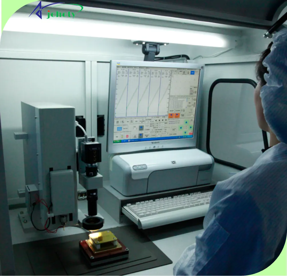
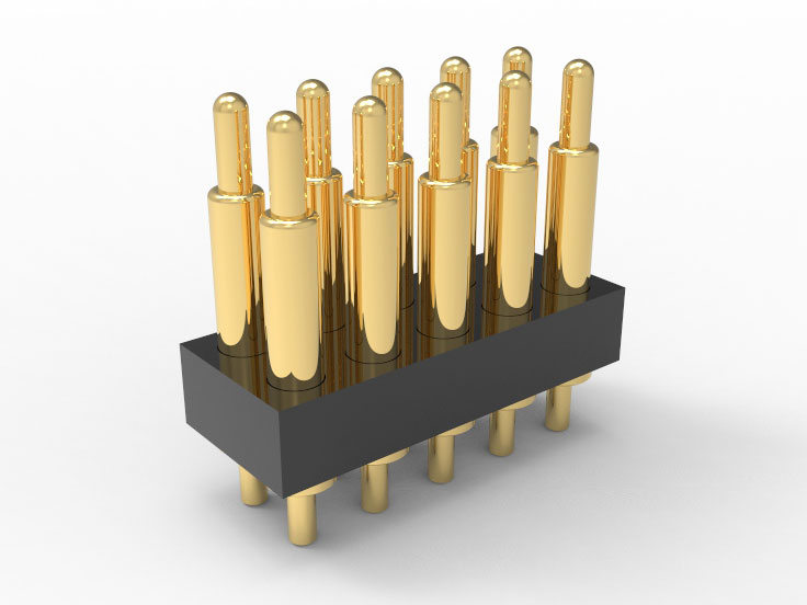
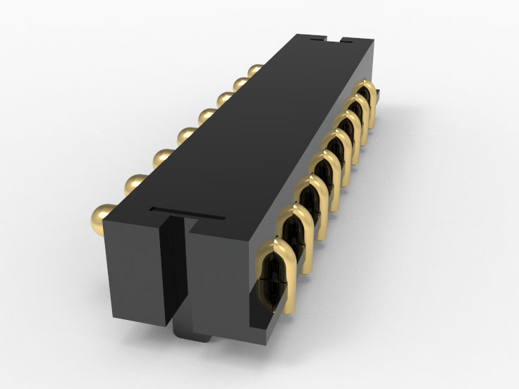
Performance Test of PCB Pins
Instantaneous resistance stability detection: Ensure that millisecond level signals are not lost during connection.
Fatigue test for connection life: Despite over 10,000 contact cycles, the impedance remains low and there is no offset.
Contact force consistency calibration: ± 0.05N precision control to avoid PCB micro damage and virtual soldering.
High frequency signal integrity scanning: Maintain S21 insertion loss<-1.2dB at 10GHz, perfectly matching high-speed design.
High and low temperature cyclic impact test: stable operation from -55°C to+125°C, without cracking or elastic attenuation.
Salt spray corrosion test passed for 96 hours: sweat resistant, oxidation resistant, and can be directly used for consumer/automotive products.
Full elasticity balanced distribution detection: 100% yield, eliminating hidden dangers such as unstable contact and spring breakage.
Surface coating X-ray analysis: controllable gold thickness ± 0.05μm, long-term wear resistance, and welding friendliness.
Automated AOI optical sorting: zero leakage of micro defects and traceable data throughout the entire process.
Click: More Catalog
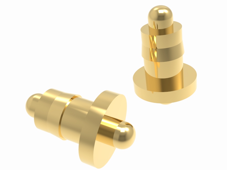
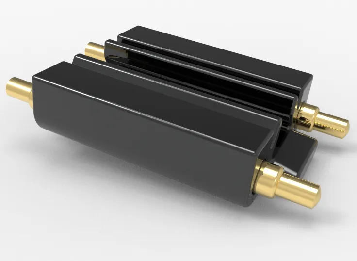
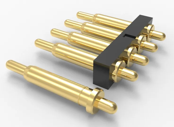
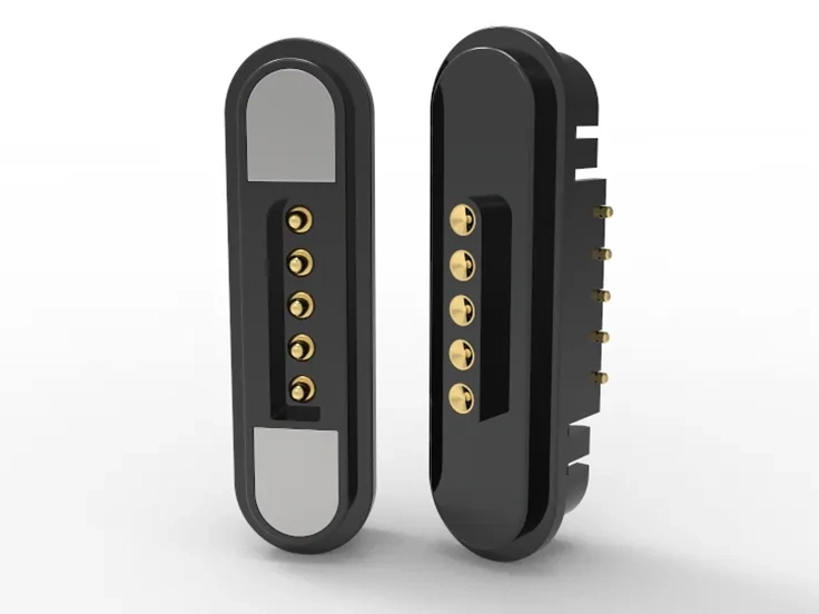
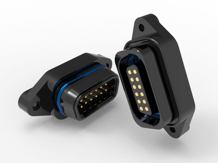
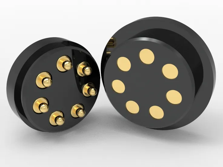
Customization of PCB Pins
Extremely low contact resistance: The contact resistance of PCB pins is ≤20mΩ, ensuring stable transmission of high-speed, high-frequency, and high-current signals.
High cycle life: Mechanical life of over 50,000 cycles, suitable for high-frequency testing, automated probe stations, and repeated connections.
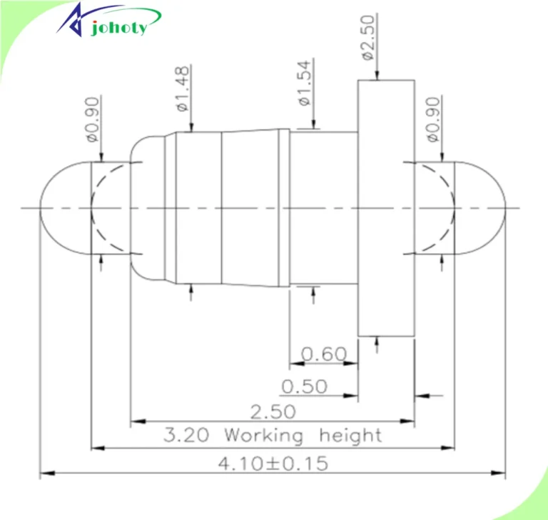
Support extreme customization: customizable shape, length of pcb pins, barrel diameter, spring force, coating, current, contact resistance, etc. Adapt to irregular spaces and non-standard connection and fixture structures.
Coating: gold/silver/nickel/palladium alloy, which meets different applications such as corrosion resistance, wear resistance, and electrical consistency.
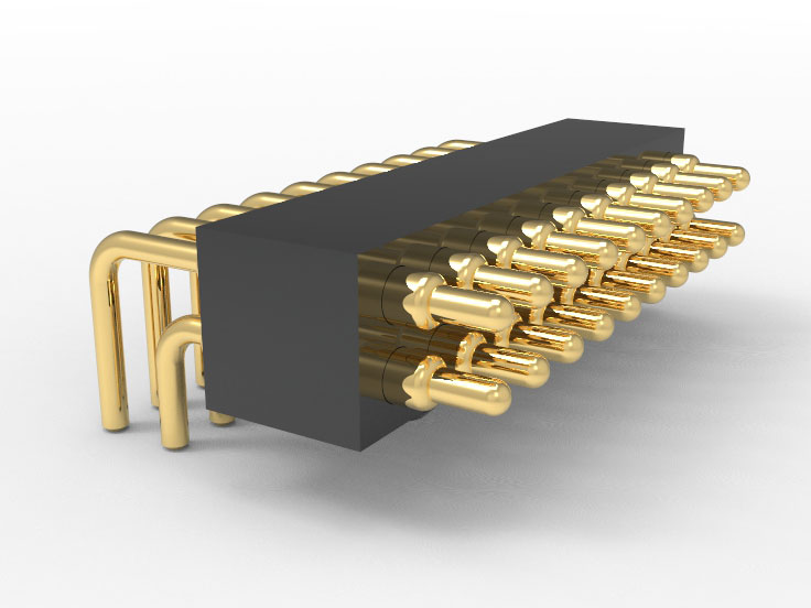
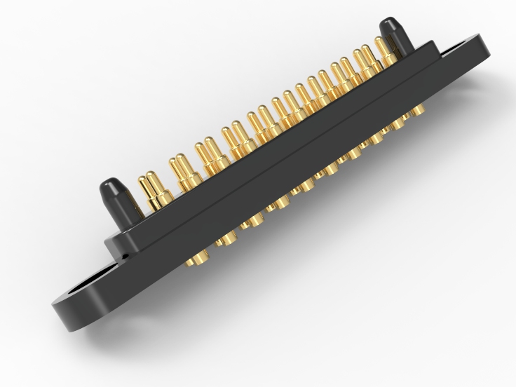
Automated compatibility design: can be embedded in various PCB board connections, used in automated testing fixtures, connector modules, FPC/PCB structures.
Reliability certification: passed multiple factory tests such as salt spray, insertion and extraction force, overload current, temperature rise, and withstand voltage.
Click: More Catalog
FAQ
Can PCB pins support high-speed signal or high current power transmission scenarios?
support. We offer a stable current design of ≥3A and have a preferred>10mΩ low resistance gold-plated pogo pin structure. Suitable for scenarios with high or medium high current requirements for signal integrity. Customers often use it for battery management systems, intelligent terminal motherboard docking, etc.
Can it replace traditional welding connectors and improve modular assembly efficiency?
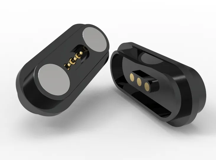
sure. The dual headed pogo pin supports solder free quick connections and is suitable for pluggable modules, hot swappable systems, and high-density stacked PCB structures, significantly simplifying the assembly process and shortening the research and development cycle.
Do PCB pins have the ability to supply in bulk and provide full process technical support?
have. We have provided stable delivery of 10K~500K levels to multiple customers in North America and Europe. Provide engineering technical support for structural sampling, selection optimization, and verification testing. From prototype, EV, DV, PM to mass production
Can PCB pins be customized in size, elasticity, and material to meet precision engineering requirements?
sure. Support full-size customization from elasticity, length of PCB pins, barrel diameter to end design. Meet industrial standards for miniaturization from 1.00mm spacing to high-speed connector level. Accurately match the strict requirements of engineers.
Are PCB pins suitable for high-speed plugging or high-frequency cycling connections?
Applicable. The cycle life of PCB pins can achieve ≥200,000 cycles, with stable elasticity and no fatigue Charging interface, module testing stand, and repeatable assembly structure for high-frequency operation.
 +86 13590816656
 +86 13590816656