Johoty’s Services of PCB Pogo Pins
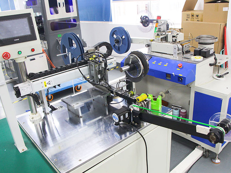
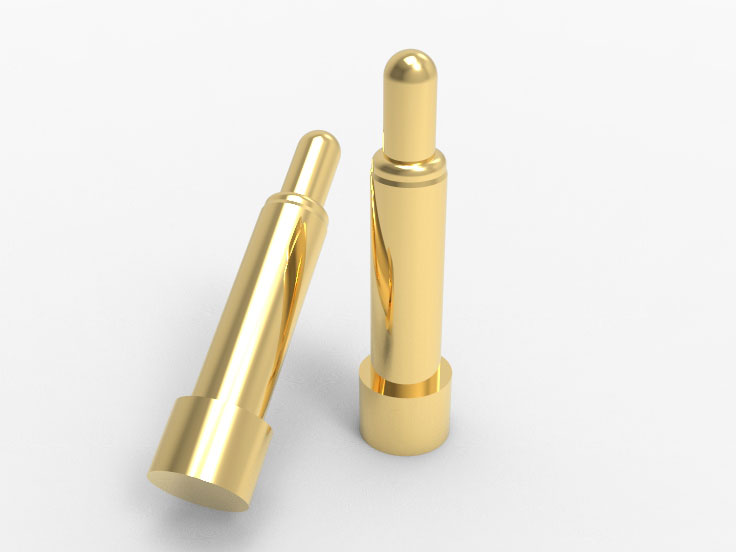
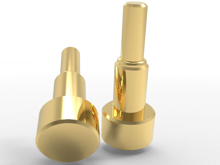
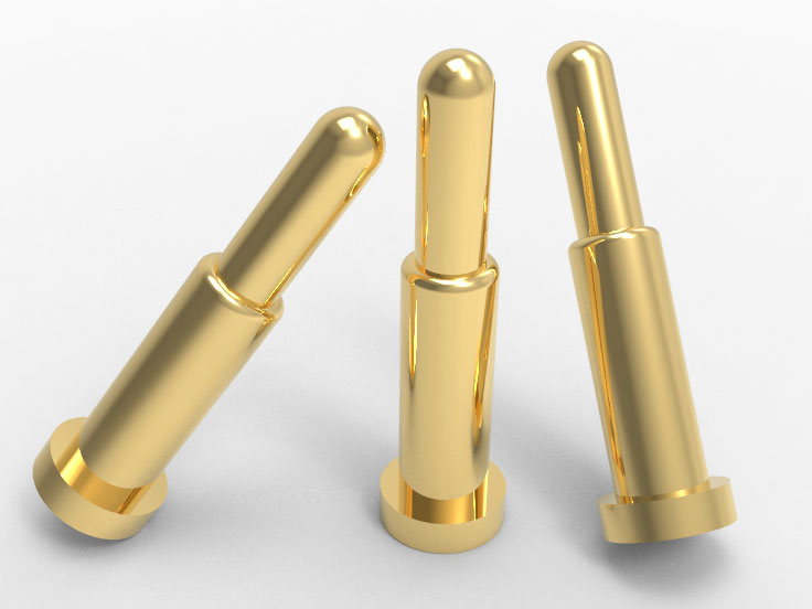
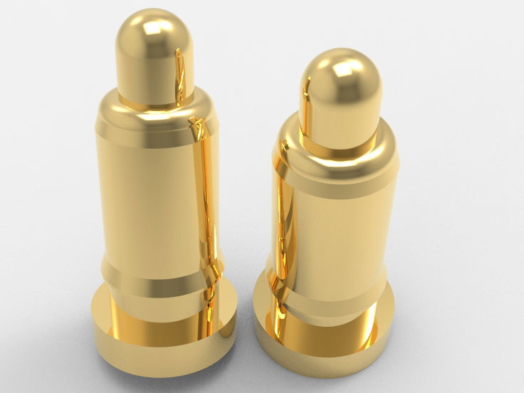
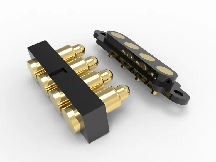
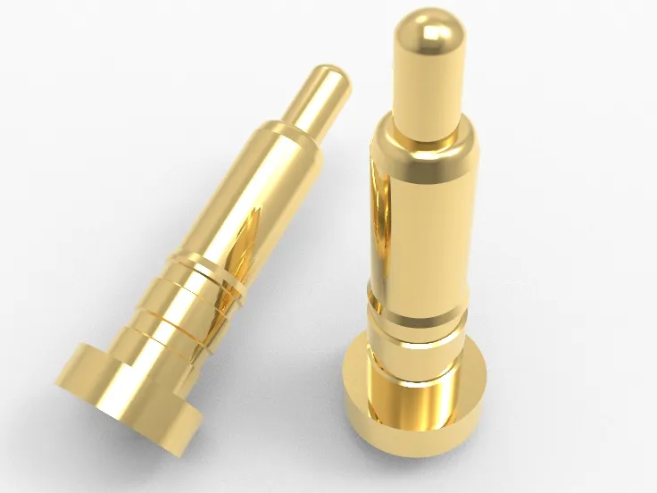
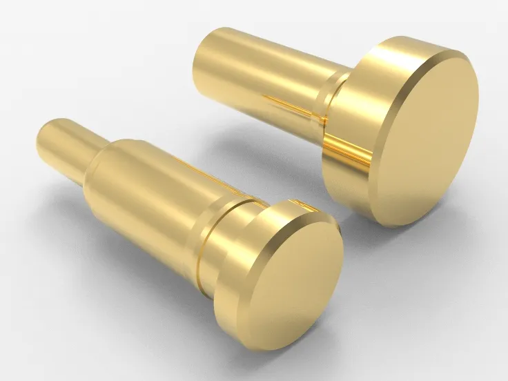
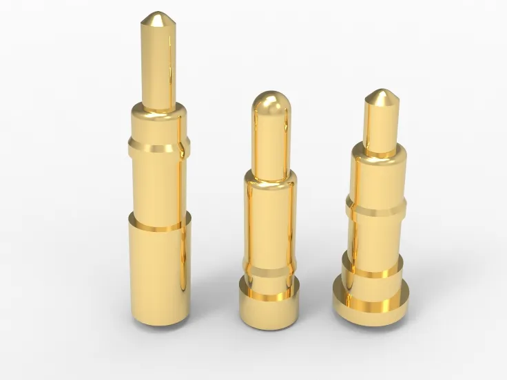
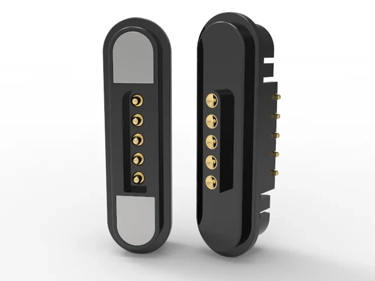
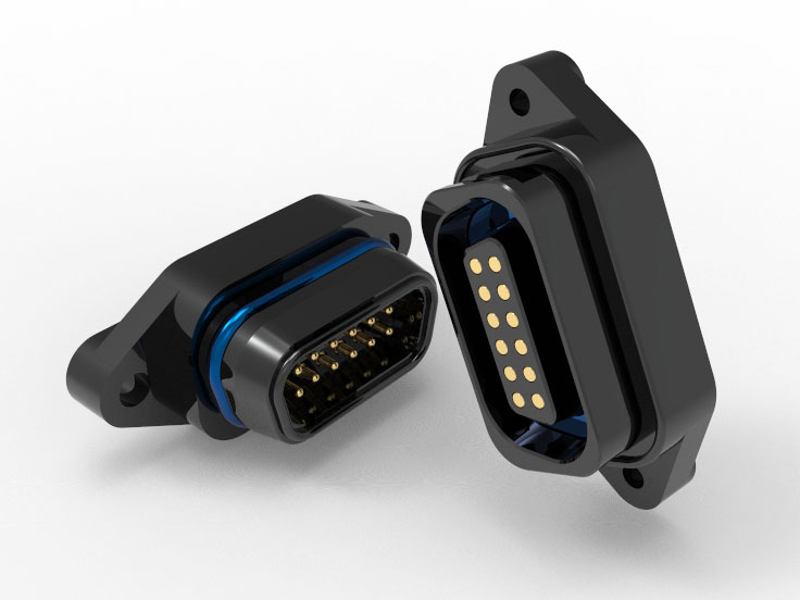
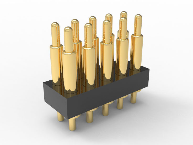
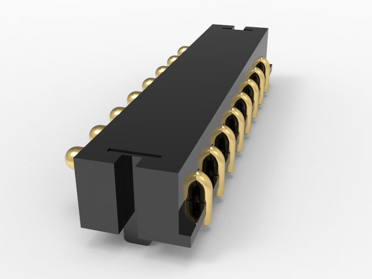
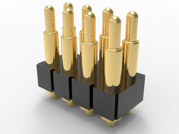
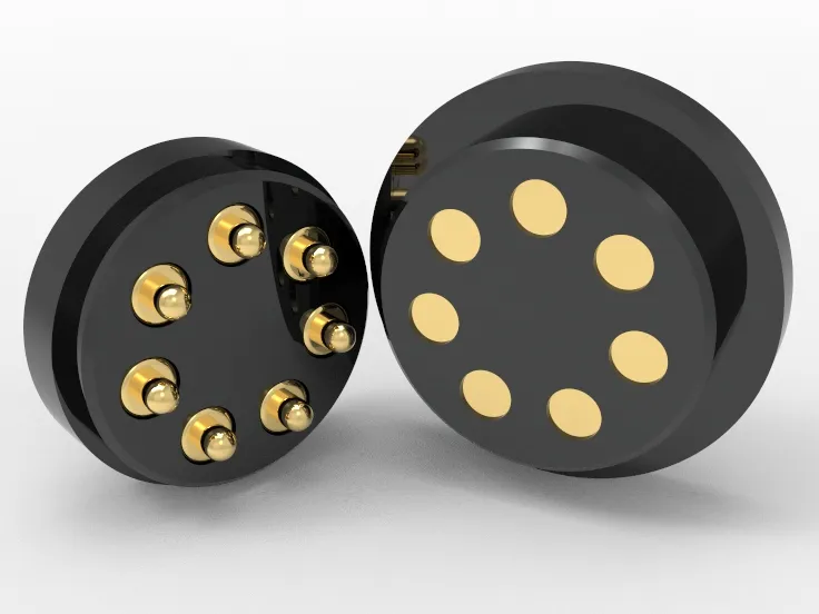
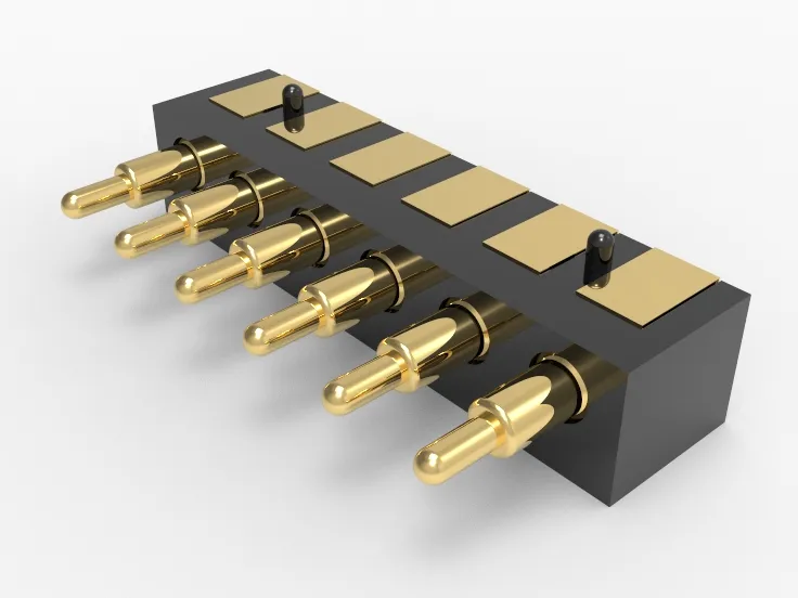
Sample PCB Pogo Pins:
Lead the entire process of engineering and connect with senior structural/process engineers. Preliminary 3D evaluation and structural recommendations should be completed within 24 hours. Provide free sample structure compatibility suggestion diagrams. The standard sampling process (Drawing → DFM → Structure → Process → Sample Production) is compressed to produce samples within 72 hours (conventional structure). Complex structure ≤2 weeks. Visualize and track the entire sampling process.
PCB Pogo Pins Quality Standards:
According to the IPC-A-610 Class 3 standard management. The coaxiality, elasticity attenuation rate, contact resistance, and average thickness of the coating at the tail of PCB pogo pins can be accessed through batch to batch inspection records. Barrel coating defaults to ≥50μ”Au over Ni and supports customization. Before leaving the factory, ≥ three rounds of simulated rebound testing>10000 times. Resistance deviation ≤ 5mΩ, complete SPC report shall be attached for each batch upon delivery.
PCB Pogo Pins delivery time:
The minimum lead time from sampling to bulk shipment for standard specifications (≤ 4types of non-customized structures) is 10 working days. If fixture/mold development is required, the delivery cycle should be estimated in advance. Project oriented customers support delivery in batches and capacity locking agreements.
Minimum Order Quantity (MOQ):
Standard structure sampling without MOQ, minimum order quantity for small batch trial production ≥100pcs, minimum order quantity for customized structure ≤500pcs. The formal mass production stage supports monthly framework agreements (including material pre investment and warehouse management mechanisms).
Logistics method of PCB Pogo Pins:
During the sampling stage, DHL/UPS/FedEx/TNT will be used by default, and global delivery will be made within 5-8 days. Formal orders can be placed FOB in Chinese ports or DAP in global cities. Provide quotes and estimated time plans for four routes: sea/air/rail/truck.
Qualification of person:
The contact person must have a background in the precision connector industry of at least 10 years and possess dual abilities in structural engineering and application engineering. Familiar with the collaboration process of FAE end and the project promotion logic of European and American communication, medical, and automotive industries. Can assist customers in completing packaging size verification/DFMEA recommendations between upstream PCBA/machine end.
Click: More Catalog
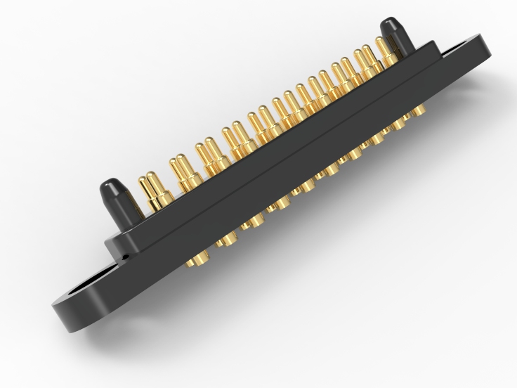
Performance Test of PCB Pogo Pins
Mating force stability test: maximum deviation <±0.15N, ensuring consistent contact performance for lengths >11.00mm. Multiple insertions and removals of the structure have been verified to be normal and the functionality is stable.
Assessment of Contact Resistance Drift: After 10,000 consecutive on-off cycles, the resistance change does not exceed 8%. Supports strict communication and high-speed data applications for signal integrity.
High temperature welding stress residual test: After reflow at 260℃, there is no structural deviation between the barrel and tail pin. It meets the high thermal impact requirements after SMT assembly.
Vertical compression deformation consistency: Under 3.00mm full stroke compression, the vertical axial offset is less than 0.03mm. The repeated positioning accuracy of the connection point is required to not exceed ± 0.05mm.
Flat bottomed solder pad suction uniformity test: The variation rate of contact area after solder paste spreading is less than 5%, which improves the stability of the welding process window in mass production.
Click: More Catalog
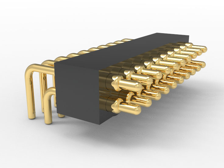
Customization of PCB Pogo Pins
Structural accuracy control: The end is designed with a flat bottom, with a length of ≥11mm, to ensure stable docking in the automatic SMT process. Avoid offset and virtual soldering, and adapt to the connection module structure with high consistency requirements.
Rare specification processing capability: supports integrated manufacturing of pogo pin structures with lengths ranging from 11.00 to 60.00mm, with a length tolerance control of ± 0.10mm. It is suitable for industrial and medical grade use that requires high compression ratio and stable insertion and extraction life >10,000 times.
Electrical performance consistency guarantee: The impedance is stable below 50mΩ and adopts a double-layer spring + thickened gold-plated structure. The current carrying capacity can reach 50A, suitable for integrated design of high-speed signal and power supply mixed channels.
Compatible with non-standard PCB pad layout: supports customized pin pitch (0.80/1.00/1.27/2.50/2.54mm, etc.). Optimizing the contact area of solder pads to enhance welding strength and reduce the risk of connection failure caused by stress concentration.
Quick verification mechanism: Complete feasibility assessment and structural drawing feedback within 48 hours of receiving the drawings, with an optional sample period starting from 72 hours. All batches pass 100% automatic testing for insertion force, rebound force, withstand voltage, and contact impedance.
Click: More Catalog
FAQ
What types of surface mount scenarios are PCB pogo pins suitable for?
The SMT process can be directly soldered to standard through-hole PCB pads. Suitable for high-frequency replacement, module elastic connection, battery holder, etc. that require high maintainability and contact reliability.
How to ensure vertical stability of PCB pogo pins with a length >11mm in SMT applications?
This structural design adopts a downward pressure self stabilization+flat bottom support mode, combined with patch adhesive assistance. PCB pogo pins are compatible with standard reflow soldering processes, without the risk of displacement or tilt.
What are the recommended PCB pogo pins pad sizes and mounting process parameters?
It is recommended to have a pad area of ≥1.5 times the diameter of the bottom surface, and to use medium to high viscosity lead-free paste. The reflux peak temperature is controlled at 245°C±5°C, which is compatible with the standard SMT line mounting cycle.
Is the spacing of PCB pogo pins controllable in high-density PCB design with multiple PIN layouts?
The minimum pin spacing support is 1.27mm pitch, with good shielding consistency and automatic mounting compatibility. PCB pogo pins adapt to modular/plug-in interface design.
Can PCB pogo pins provide high-frequency/high current operation verification data?
PCB pogo pins support <20mΩ contact resistance and >10,000 plug and unplug cycles. The maximum passing current reaches 3.0A at room temperature, accompanied by a standard current carrying curve and impedance stability test report.
 +86 13590816656
 +86 13590816656